PCB Design and Fabrication
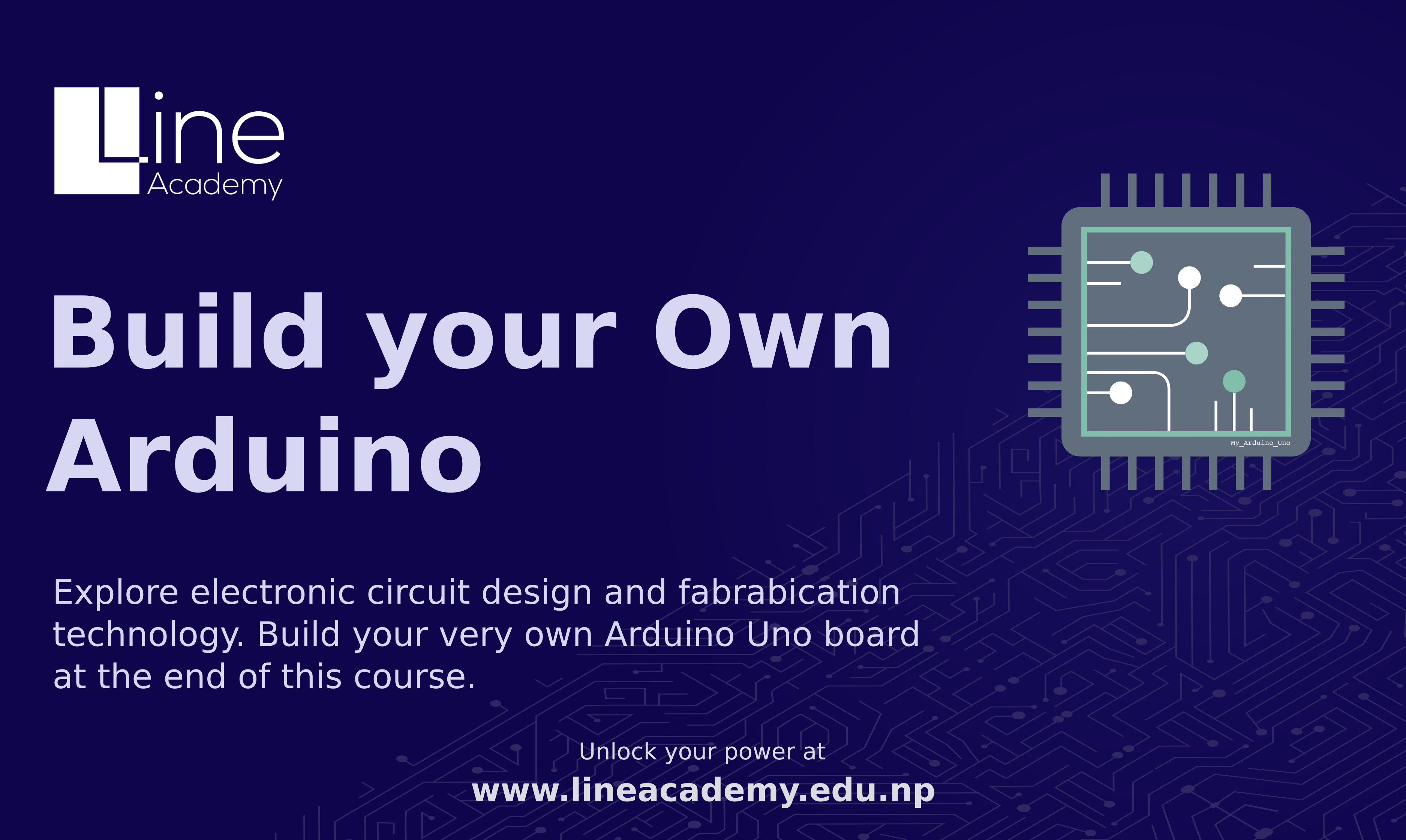
This course is designed for students to explore electronics circuit design and fabrication technology. The course aims to do so by teaching students various principles of circuit design and pcb design/fabrication by creating a very own Arduino Uno clone. Students will create schematic and design PCB layout on KiCad while getting insights on various design philosophy. At the end students will have their own arduino clone and enough knowledge to create commercial grade electronic circuits and PCB’s.
Course Structure
The course is designed into two sections. The first section provide introduction to KiCad and it’s features. Meanwhile second section will provide in depth knowledge about circuit design. The whole course is scheduled for two week’s while each segment taking one week. During first section students will get familiar to KiCad interface, KiCad Project, Schematic capture in KiCad and PCB design in KiCad. Student’s will learn this while creating a atmega32 based AVR development board. This section will also provide information on KiCad libraries, footprints and 3D Model of designs. During second section student’s will get familiar with electronic fabrication project and will learn various steps of planning, starting and closing a project. Student’s will learn how to draw good schematic, create a component, create a footprint, laying out PCB and routing. The whole course is designed to be practical and interaction oriented. Student’s will be actively participating throughout the course.
Syllabus
- Class 1: Introduction to Tutor, Introduction to Course, installation of required softwares and basic introduction to circuit design.
- Class 2: Introduction to KiCad. Planning and creating a Atmega32 development board project. Introduction to KiCad Schematic and libraries.
Drawing schematic for Atmega 32 development board. - Class 3: Continuation to KiCad Schematic and libraries.
Drawing schematic for Atmega 32 development board. - Class 4: Introduction to KiCad PCBnew and footprints.
Creating PCB layout for Atmega 32 development board. - Class 5: Continuation to KiCad PCBnew and footprints.
Creating PCB layout for Atmega 32 development board. - Class 6: Single layer PCB Home fabrication techniques Demonstration.
- Class 7: Schematic Capture, do’s and dont’s. Good Practices.
Starting project and Schematic capture for Arduino uno Clone. - Class 8: Schematic Capture, Making good schematic better.
Schematic capture for Arduino uno Clone. - Class 9: Selecting components. Price, size, availability and other constraints.
- Class 10: PCB layout, Placing components, do’s and dont’s of PCB layout.
Starting PCB layout of Arduino Uno Clone. - Class 11: PCB layout, Routing, do’s and dont’s of PCB routing.
PCB layout of Arduino Uno Clone. - Class 12: Finaizing design and preparing for fabrication. BOM and Gerber file generation.
Overview of PCB fabrication technique. Sending board for fabrication.